
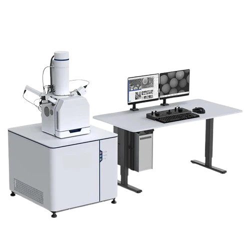
SE 300000x Scanning Electron Microscope (SEM) | High-Resolution Imaging AM637032
by MEUBON
Save 8%
Original price
$435,717.00
Original price
$435,717.00
-
Original price
$435,717.00
Original price
$435,717.00
Current price
$400,000.00
$400,000.00
-
$400,000.00
Current price
$400,000.00
SE 300000x Scanning Electron Microscope (SEM)
Specifications:
-
Resolution:
- 3.9nm @20kV (SE), 4.5nm @20kV (BSE)
- 3nm @30kV (SE), 4nm @30kV (BSE)
- 8nm @3kV (SE), 1.0nm @15kV (SE)
- 1.5nm @1kV (SE), 0.8nm @30kV (STEM)
-
Voltage:
- Standard: 0.5kV to 20kV
- Optional: Up to 30kV
- 20V to 30kV available on select models
-
Magnification:
- 1x to 300,000x
- Film: 1x to 300,000x
- Screen: 1x to 1,000,000x
- Extended: 1x to 2,500,000x
-
Electron Gun:
- Pre-Aligned Tungsten Filament (Standard)
- Schottky Field Emission Electron Gun with in-cylinder deceleration, electromagnetic composite objective, and water-cooled thermostatic objective (Advanced Model)
-
Vacuum System:
- Fully automated, oil-free vacuum system
- <5×10⁻⁴ Pa standard vacuum level
- Optional low vacuum capability (5 to 1000 Pa)
- Advanced Model: Electron Gun vacuum <9x10⁻⁸ Pa; Sample Room <5x10⁻⁴ Pa
-
Vacuum Pumps:
- Mechanical Pump: >200 L/min or >6m³/h
- Turbo Molecular Pump: >240 L/S
- Advanced Model: Includes Ion Pump x2, >25 L/s
-
Working Stage:
- 2-Axis Auto Stage (X: 100mm, Y: 100mm)
- 5-Axis Auto Stage (X: 120mm, Y: 115mm, Z: 50mm, Tilt: -10° to +90°, Rotation: 360°)
- Optional 3-Axis Auto Stage
-
Camera:
- Vertical Optical Navigation CCD (Standard)
- Horizontal Monitoring CCD (Advanced Models)
-
Detectors:
- Secondary Electron Detector (ETD)
- High Angle Electron Detector Inlens (Advanced Model)
-
Software:
- SEM Operation Software with multi-channel display, optical navigation, gesture navigation, auto brightness/contrast, autofocus, auto astigmatism
- Supports image formats: TIFF, JPG, BMP, PNG
- Language options: Chinese/English
-
Computer System:
- Workstation with 16GB memory, 512GB hard disk, 24" monitor, Windows 10
-
Installation Requirements:
- Room dimensions: L >3000mm, W >4000mm, H >2300mm
- Temperature: 20~25°C, Humidity: <50%
-
Power Supply:
- AC 220V (±10%), 50Hz, 2kVA
Optional Accessories:
- Backscatter Electron Detector (BSE)
- Energy Dispersive X-ray Spectroscopy (EDS)
- Electron Backscatter Diffraction (EBSD)
- STEM, 9-quadrant, total area 80mm²
- Electron Beam Induced Current (EBIC)
- Cathodoluminescence (CL)
- Knob Control Panel & Trackball
- Sample Exchange Warehouse
- Beam Gate & Electron Beam Exposure
- Low Vacuum Detector (LVD)
- Double Anode (Tetrode Emission)
- Tungsten Filament (6pcs)
- Large Size Image Stitching Software
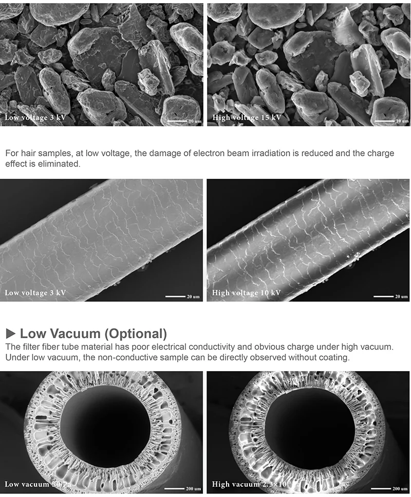
▶ Low Voltage
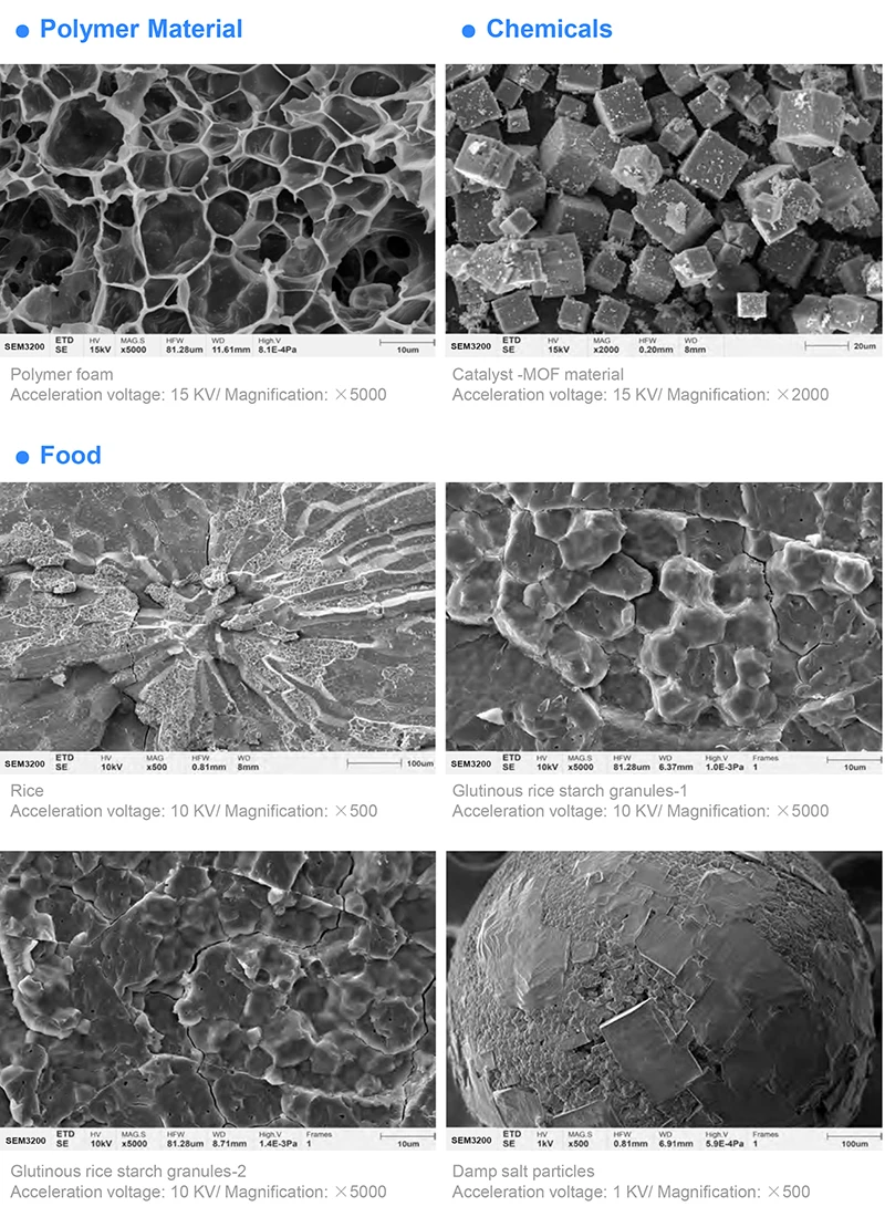
For carbon material samples, at low voltage, the penetration depth is small, and the true morphology of the sample surface can be obtained with richer details.
For carbon material samples, at low voltage, the penetration depth is small, and the true morphology of the sample surface can be obtained with richer details.
This SEM offers unparalleled imaging capabilities with a resolution of up to 0.8nm and magnification up to 2,500,000x. The advanced vacuum system, high-precision electron gun, and fully automated stage make it ideal for high-resolution research and analysis in a variety of scientific fields. With customizable accessories and software options, this SEM is adaptable to your specific research needs.
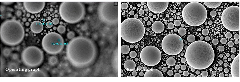
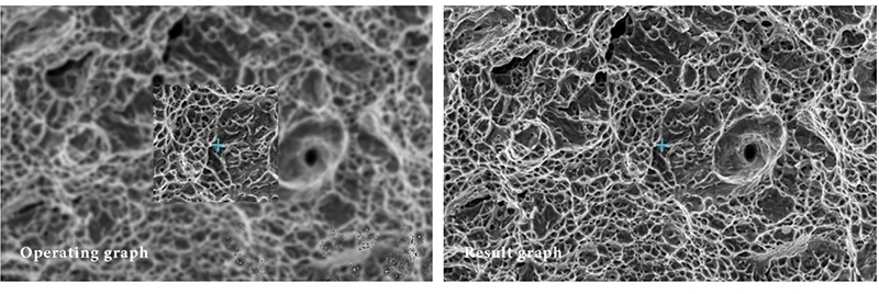
▶ Feature Function
Intelligent Assisted Astigmatism
Directly reflect the astigmatism of the whole field of vision, through the mouse click clear, can quickly adjust the astigmatism to the best.
Intelligent Assisted Astigmatism
Directly reflect the astigmatism of the whole field of vision, through the mouse click clear, can quickly adjust the astigmatism to the best.
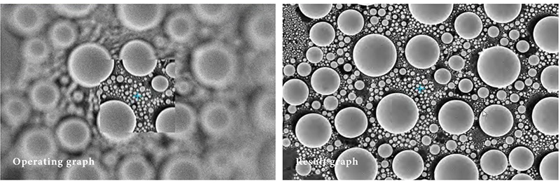
Autofocus
One-click focus for fast imaging.
One-click focus for fast imaging.
Automatic Astigmatism
One-click astigmatism, improve efficiency.
One-click astigmatism, improve efficiency.
Automatic Brightness Contrast
One-click automatic brightness contrast, gray level appropriate image.
One-click automatic brightness contrast, gray level appropriate image.
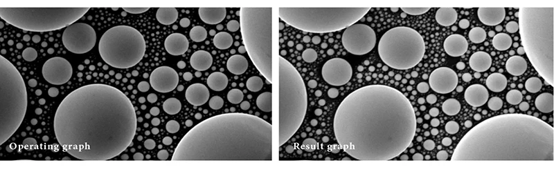
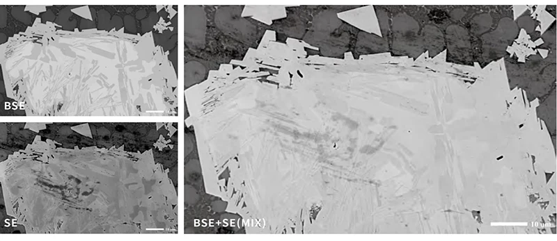
Image Multiple Information Simultaneously
A63.7032 supports one-click switching between SE and BSE hybrid imaging, the morphology and composition information of samples can be observed simultaneously.
A63.7032 supports one-click switching between SE and BSE hybrid imaging, the morphology and composition information of samples can be observed simultaneously.
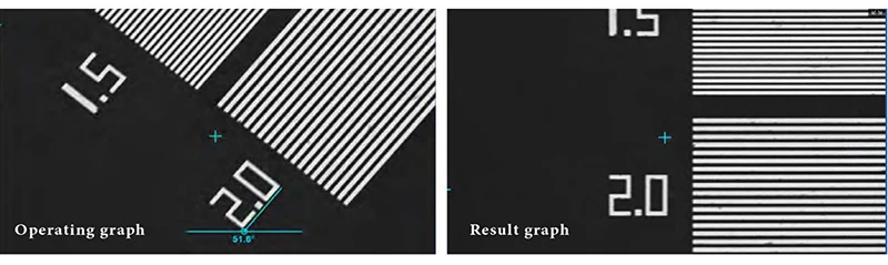
Fast image Rotation
Drag a line and the image is instantly "angled“.
Drag a line and the image is instantly "angled“.

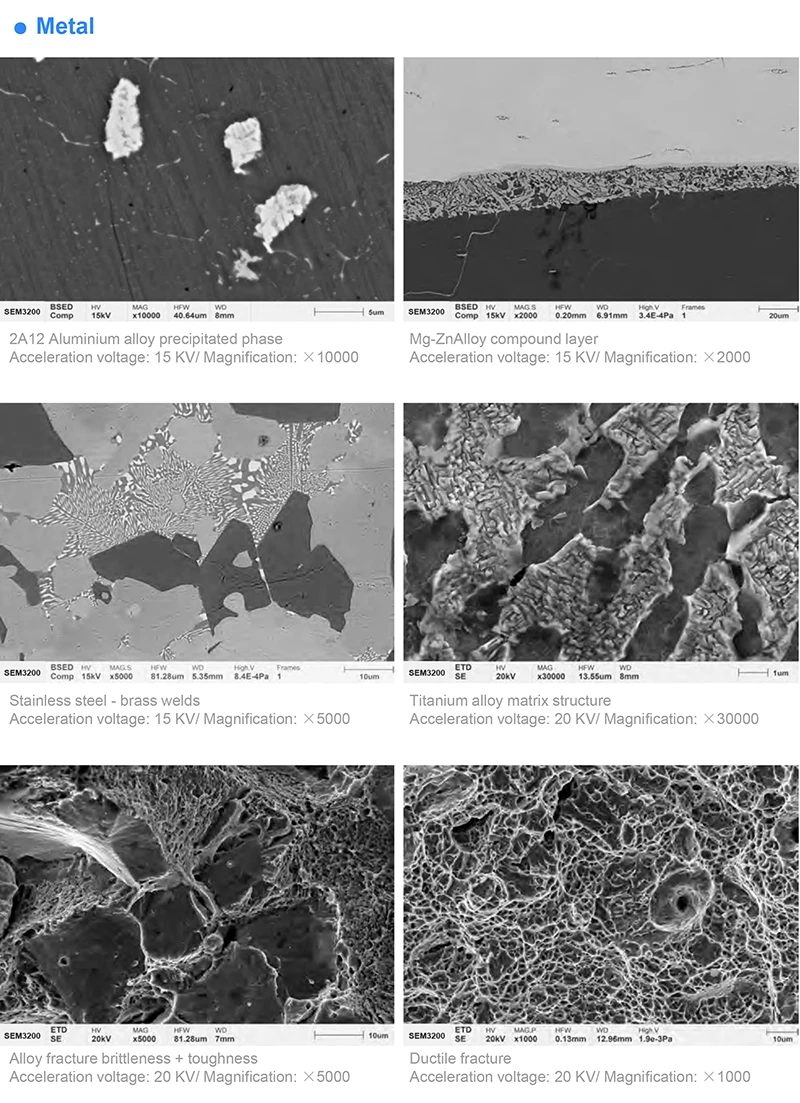
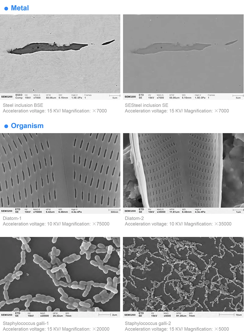
Scanning electron microscope is not only limited to the observation of surface morphology, but also can be used to analyze the micro-components of the sample surface.
In addition to conventional secondary electron detector (ETD), backscattered electron detector (BSED), and X-ray energy dispersive spectrometer (EDS), many interfaces are reserved, such as electron backscattered diffraction (EBSD), cathode ray (CL) detectors can be integrated on A63.7032.
In addition to conventional secondary electron detector (ETD), backscattered electron detector (BSED), and X-ray energy dispersive spectrometer (EDS), many interfaces are reserved, such as electron backscattered diffraction (EBSD), cathode ray (CL) detectors can be integrated on A63.7032.
Quadripartite Backscattered Electron Detector (BSE)
-- Multichannel Imaging
The detector is exquisitely designed and highly sensitive. It adopts a 4-segment design, and can obtain shadow images and component distribution images in different directions without tilting the sample
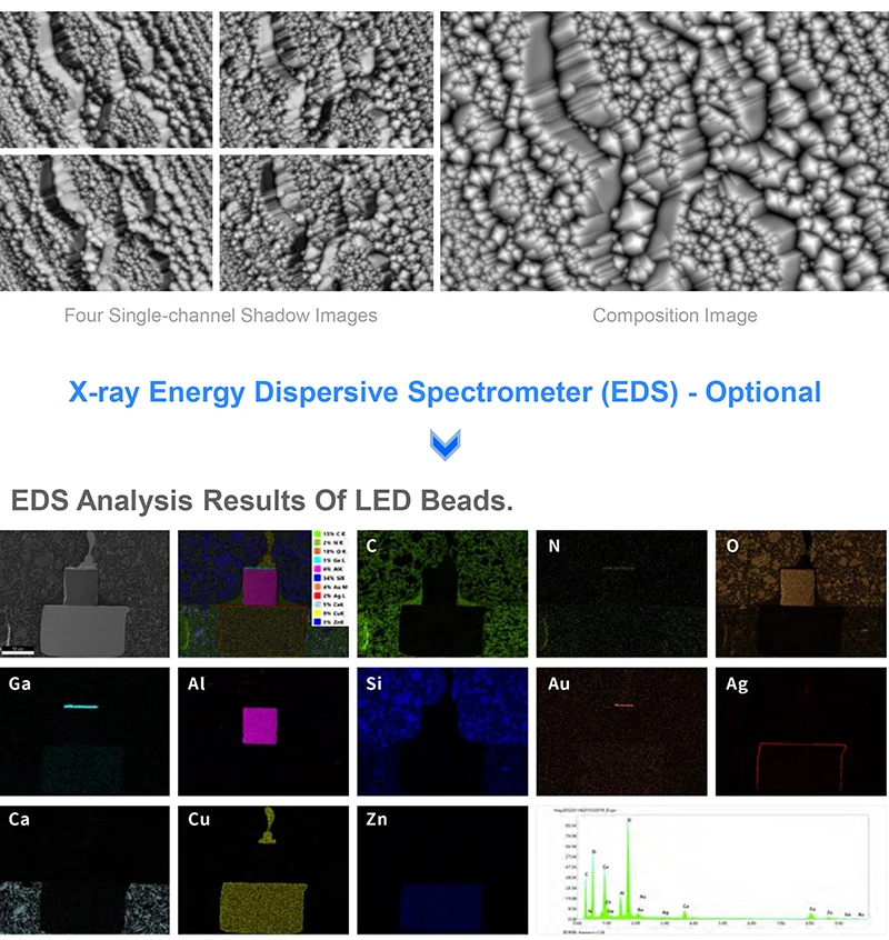

SE image VS BSE image
In the backscattered electron imaging mode, the charge effect is weakened obviously, and more composition information can be obtained on the sample surface
- Warranty : 3 years
- Model Number : AM637032
- Theory : Scanning Electron Microscope
- Drawtube : N/A
- Resolution : "3nm @30kV(SE) 4nm @30kV(BSE) 8nm @3kV(SE)"
- Voltage : 0.2kV~30kV
- Magnification : "1x~300,000x(film) 1x~1,000,000x(screen)"
- Electron Gun : Pre-Aligned Tungsten Filament
- Vacuum System : "Fully Auto Control Oil Free Vacuum <5x10⁻⁴ Pa"
- Camera : "Vertical Optical Navigation CCD Horizontal Monitoring CCD"